Translated with www.DeepL.com/Translator (free version)
Introduction
Game Boy is a word that I believe must evoke many childhood memories of the post-80s and post-90s. From simple bricks to Pokemon and The Legend of Zelda, there have been too many classic works on this platform. The Game Boy itself was produced from 1989 until 2009, with total sales of over 100 million units, making it the second best-selling handheld game console in history. It is worth pointing out that although the Game Boy was produced until 2009, its main structure is closer to the popular 8-bit game consoles such as FC (Red and White) in the 80s. The huge sales made it one of the most readily available 8-bit retro consoles. This feature attracted many players who love the unique audio and visual experience of 8-bit games to buy and play Game Boy, and also attracted many independent game developers. To this day, there are still enthusiasts who are developing new games for the Game Boy platform. This feature of Game Boy is not only attractive to gamers. As an 8-bit machine, the Game Boy's built-in quadraphonic PSG (Programmable Sound Generator) can generate Chiptune, the 8-bit machine's unique sound. The simple structure of the 8-bit machine itself makes it easy to understand, making the Game Boy a popular example for use in some college classes. For example, Georgia Tech University has a Game Boy game design course to help students learn to understand computer architecture, and Carnegie Mellon University has designed a Game Boy as one of the course design options for its Advanced Digital Systems Design course. All of this, occurring nearly 10 years after its discontinuation, is a testament to the powerful vitality of this classic platform.
To play Game Boy games, of course, you need a Game Boy and a game cassette. If the game you want to play is a former commercial game, then you just need to buy a used cassette. But if the game (or program) is homemade by a hobbyist, or if you want to run a game you wrote on the Game Boy, it's not as easy. Generally speaking, commercial game cassettes are readable but not writable, and in order to write your own games, you need a Game Boy burner card that can write.
There are some off-the-shelf burner cards available on the market today, however, they are expensive, usually more than several times the price of the Game Boy itself. However, the good thing is that Game Boy technical information is easily available online and it is possible to design and create a burner card yourself if you understand the principles.
Theory
A Game Boy cassette is a device that is used to store data. To make a cassette, you need to study the interface and protocol. The good thing is that, as mentioned above, the overall architecture of the Game Boy is very close to that of the 8-bit machines of the 80s, and there are not too many complicated things inside.
It is not difficult to find the pinout of the Game Boy's cassette interface by searching the Internet, as shown in the following table.
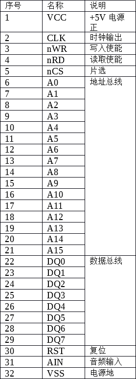
As you can see, the main signals are a set of address bus and data bus. Those familiar with microcontrollers may have noticed that these signals are close to what is generally referred to as the 8080 bus. In fact, the Game Boy uses an 8080-compatible processor, so it's no surprise.
The Game Boy has two types of operations for cassette tapes, one for reading and one for writing, which are controlled by the nRD signal and the nWR signal respectively. When the nRD signal is active (i.e. nRD is low), the Game Boy reads data from the cassette, while when the nWR signal is active, the Game Boy writes data to the cassette. Because the Game Boy's cassette interface does not have multiplexed address and data lines, it is a separate set of 16-bit address buses and a separate set of 8-bit data buses, so no additional circuitry is required to connect a simple ROM, just connect the corresponding signals to it. The memory on the cassette outputs or reads data to or from the data line according to the nRD or nWR signal.
So all you need on the cassette is a ROM chip and then you connect the wires and you're done? Not exactly. The simplest cassette does require only one ROM, but the drawback is obvious: the capacity of the Game Boy cassette slot provides a total of 16-bit address lines, which means a maximum of 2^16=65536 addresses, multiplied by 8 bits (one byte) of the data line, which can only address a maximum of 64KB of memory. However, this bus is not exclusive to ROM, but is shared by all parts of the system. Internal memory, peripheral registers, video memory, and other things are also on this bus. The total space allocated to the ROM is only 32KB. there are indeed some games that only need 32KB, such as Tetris, but most games need more space, such as The Legend of Zelda: Dreamland DX, which requires 8MB of space.
So how to solve this problem? This problem is actually a very common problem in computer systems, and the Game Boy uses a very conventional solution, paging. Simply put, there is a controller inside the cassette that can be responsible for taking out a portion of the total ROM space and mapping it to the limited 32KB address space. This controller is called Memory Bank Controller (MBC) by Nintendo, and an important part of our homemade burner card is to simulate an MBC to complete the work of memory paging.
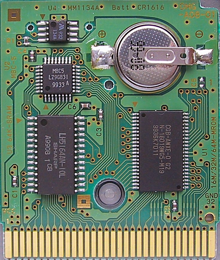
MBC is on the upper left
Before we start, let's talk about the specific implementation of MBC paging. the address of MBC on the bus is duplicated with ROM, all write operations to ROM location will be received by MBC and read operations will be received by ROM (because ROM does not need to write and MBC does not need to read, so it can share the address.) The address low bits of the ROM (A13-A0 total 14 bits, 16KB) are directly connected to the address bus, while the address high bits of the ROM (A22-A14 total 9 bits, 512 pages) are connected to the MBC. The host can write the number of pages to be selected to the MBC, and the MBC will output the corresponding address. (Actually, it is also 9 D flip-flops.) Other functions of MBC are RAM paging (works similar to ROM, used to provide paging function for RAM on the cassette), RTC timing, etc.
Overall solution
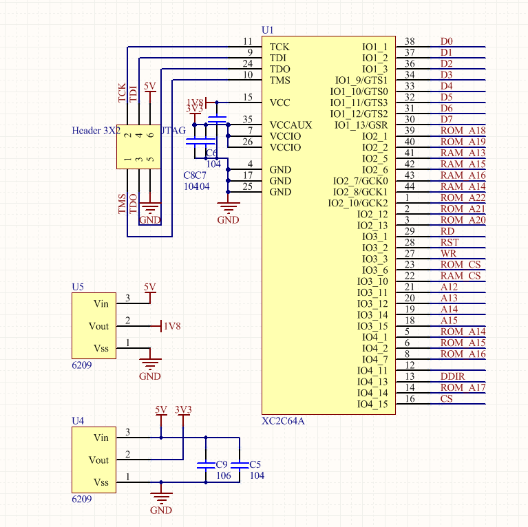
To implement the functions of the MBC, there are two options, one is to use a microcontroller simulation, the other is to use CPLD implementation. Microcontroller emulation requires the microcontroller to be fast enough to input and output data in time to complete the simulation of MBC behavior. CPLD implementation, on the other hand, does not require much because the logic is simple enough and usually the smallest size CPLD can meet the requirements. And considering that GB is a battery-powered device, the cassette should be as power-efficient as possible. the MBC itself can work without a clock, and using CPLD to implement the logic can achieve lower power consumption than the analog logic of a high-frequency microcontroller. For this reason the CPLD chosen for this design is implemented. I chose Xilinx's XC2C32A CPLD, which is the smallest logic size in the Cool Runner-II product line, with only 32 macro cells, but it is sufficient.
The Game Boy uses 5V levels, while the CPLD is at 3.3V IO levels, and ROM and RAM are also typically at 3.3V IO levels. For this reason, a more reasonable solution is to design the whole circuit as 3.3V, and add bus drivers to the interface section to achieve level conversion.
Circuit design
The overall design is not too special, just as planned, with the bus driver connected at the interface for level conversion. Note that the RST signal is not output from the Game Boy to the cassette, but from the cassette to the Game Boy. if the Game Boy is not to be reset, this pin should be left floating and should not be used to reset the components on the cassette. ain and clk are not used.
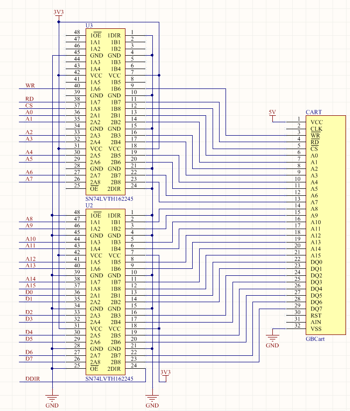
RAM and ROM should connect directly to GameBoy as described (here that's bus driver) RAM和ROM部分也和描述一样,数据线直接和Game Boy相连(这里是总线驱动器输入/输出)
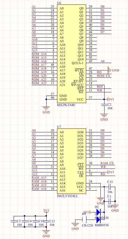
The CPLD part is connected to the RAM and ROM address high, Game Boy output control signal, data bus and part of the address bus (Nintendo's design MBC is only part of the address line, after all, MBC itself is not too many registers can be adjusted.) CPLD needs a 1.8V core voltage in addition to the 3.3V IO voltage, also using an LDO to provide. cpld burn program through the JTAG interface, remember to leave a good pad or test point.
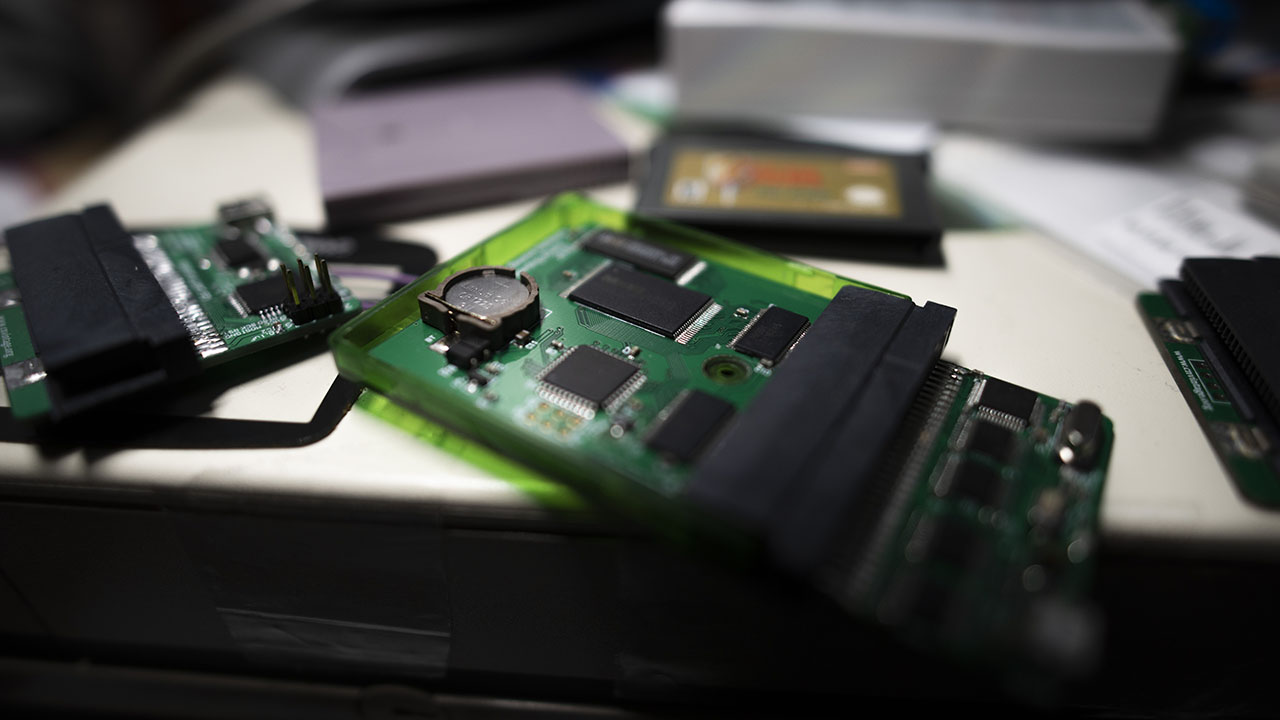
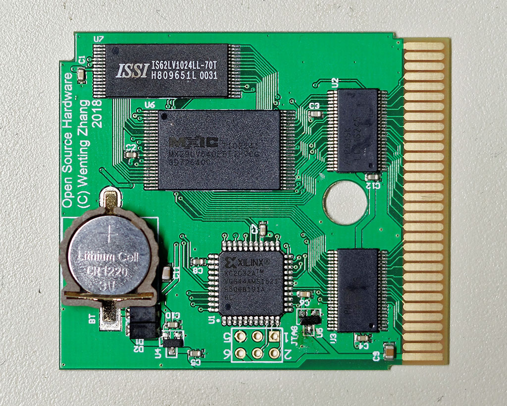
The finished PCB:
CPLD design
Generally speaking, there are two ways to design the internal logic of a CPLD: one is to draw a schematic directly and use logic gates to represent the logic to be implemented; the other is to use a hardware description language (HDL) to describe the logic to be implemented through code. Here I use Verilog language to implement the logic of MBC.
The first step is to implement ROM paging by writing the corresponding address into a register and outputting the register contents to the high bit of the ROM address line. Note that the paging area is only the high 16KB of the 32KB space and the low 16KB is the fixed page 0. For this reason, the paging output should be disabled when the host is detected reading the low 16 bits.
reg [8:0] rom_bank = 9'b000000001; // High 16K maps to page 1 by default

wire [15:0] gb_addr = { GB_A[15:12], 12'b0 };
wire rom_addr_en = (gb_addr >= 16'h0000)&(gb_addr <= 16'h7FFF); // Current address is in ROM range
wire rom_addr_lo = (gb_addr >= 16'h0000)&(gb_addr <= 16'h3FFF); // Current address is in lower 16K

wire rom_bank_lo_clk = (!GB_WR) & (gb_addr == 16'h2000); // Host write ROM paging high
wire rom_bank_hi_clk = (!GB_WR) & (gb_addr == 16'h3000); // Host write ROM paging low

always@(negedge rom_bank_lo_clk)
begin
  rom_bank[7:0] <= GB_D[7:0];
end

always@(negedge rom_bank_hi_clk)
begin
  rom_bank[8] <= GB_D[0];
end

assign ROM_A[22:14] = rom_addr_lo ? 9'b0 : rom_bank[8:0]; // Output ROM high address
assign ROM_CS = ((rom_addr_en) & (GB_RST == 1)) ? 0 : 1; // Output ROM CS
RAM paging is similar, except it has a bit for disabling RAM access.
wire ram_addr_en = (gb_addr >= 16'hA000)&(gb_addr <= 16'hBFFF); // Current address is in RAM range

wire ram_bank_clk = (!GB_WR) & ((gb_addr == 16'h4000) | (gb_addr == 16'h5000)); // Host write to RAM paging
wire ram_en_clk = (!GB_WR) & ((gb_addr == 16'h0000) | (gb_addr == 16'h1000)); // Host write to RAM enable

always@(negedge ram_bank_clk)
begin
  ram_bank[3:0] <= GB_D[3:0];
end

always@(negedge ram_en_clk)
begin
  ram_en <= (GB_D[3:0] == 4'hA) ? 1 : 0;
end

assign RAM_A[16:13] = ram_bank[3:0]; // Output RAM high address
assign RAM_CS = ((ram_addr_en) & (ram_en) & (GB_RST == 1)) ? 0 : 1; // Output RAM CS
So the MBC is implemented. As I mentioned I have added a bus driver to do the voltage translation, and itself requires an additional signal for controlling the direction (from cartridge to gameboy or other way around). This is not hard to handle either:
assign DDIR = (((!ROM_CS) | (!RAM_CS)) & (!GB_RD)) ? 1 : 0; // Bus driver direction
Now the CPLD part is done. 27 out of 32 macrocells are used.
Debugging & Result
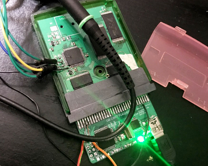
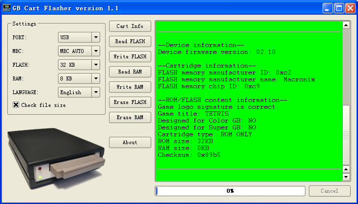
Testing with a flasher:
Flashing a game:
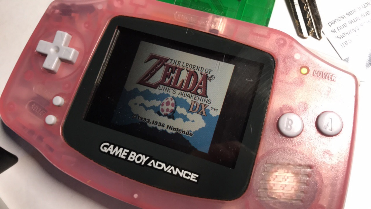
Now done.
Schematics, PCB source files, and CPLD source code could be found at: https://github.com/zephray/NekoCart-GB
Note: Game Boy, Pokemon, Legend of Zelda are registered trademark of Nintendo.